Researchers Develop Electron Nanofabrication Method Using Ice

Chinese researchers from Zhejiang University in China have created an improved 3D nanofabrication method which uses ice and electron beam technology. The method cuts down on the time it takes to develop structures using standard e-beam lithography.
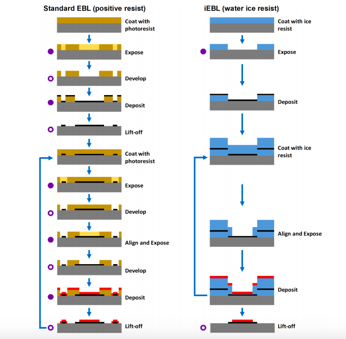
Electron beam lithography is a technique which is used to produce small electronic components. However, the standard process takes ten individual steps and a lot of time.
But, researchers from Zhejiang University in China are combining ice and electron beam technology to develop the new iEBL method of 3D nanofabrication which cuts down on these steps.
The hope is that by simplifying the technique, 3D nanofabrication will be easily accessible to other researchers and potentially used to improve electronics or medicine.
The paper, titled “Three-dimensional in situ Electron Beam Lithography Using Water Ice,” begins by explaining that all experiments are performed in a dedicated vacuum system.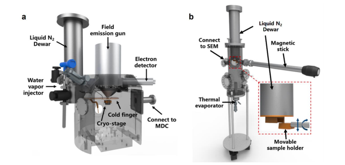
The Basics on How the iEBL Method Works
The researchers explain that their system includes “a modified Zeiss Sigma field emission scanning microscope (SEM) with a liquid-nitrogen dewar, a water vapor injector, an airlock chamber and a metal deposition chamber.”
In the vacuum, which is kept at minus 130 degrees Celsius (or minus 266 degrees Fahrenheit), water vapor turns to ice. From this, the researchers can construct 3D metal structures.
With the Zhejiang University’s iEBL method, the ice precedes a layer of metal film. Then, a layer is cut out of the ice using an electron beam.
The researchers add that they reduced the time it takes to 3D print a nanopyramid using their method when compared to the standard EBL method by twenty minutes. As well as requiring fewer processing steps and cutting down on time, this method also is contamination-free.
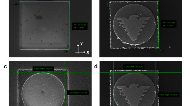
According to the researchers, their method can achieve a pattern resolution of 20 nanometers and an alignment error below 100 nanometers.
If you want to find out more about the details, make sure to read the researcher’s paper, here.
Source: China Daily
License: The text of "Researchers Develop Electron Nanofabrication Method Using Ice" by All3DP is licensed under a Creative Commons Attribution 4.0 International License.