Nano Dimension: 3D Printing Multi-material Electrical Conductors

Nano Dimension – a leading printing electronics company in the area of 3D printing – announced that they filed a patent application with the US Patent and Trademark Office for the printing of 3D models, including electronic conductors.
The Israel based company, founded in 2012, made their name as the developers of 3D printing electronics systems and nanoparticle 3D printing inks. They are now working on a method of 3D printing multi-material objects, including electrical conductors and other 3D objects with conductive traces.
What Does Nano Dimension’s Development Mean for 3D Printing?
Well, creating functional electronics straight out of a 3D printer can open up so many fields from consumer electronics to military applications. For items which require controlled and careful processes, such as missiles and smartphones, individual materials need to be fabricated.
However, a precise multi-material 3D printing process would completely change the game. Being able to embed connectors directly into electronic circuits eliminates the need for assembling sensitive parts.
This would mean that creating complex electronic circuits would be much easier and save both time and money for manufacturers.
How Does It Work?

Nano Dimension’s multi-material 3D printing involves the sintering of a printed metal conductor within a 3D printed polymer, which allows for complex connectors to be 3D printed, making it possible to 3D print molded connectors directly onto the electronic circuits.
The company claims on their website that the process can also be applied to 3D printing non-flat electronic circuits as well as structural objects with embedded electronic circuits.
Hopefully, this 3D printing breakthrough will enable manufacturers to create freeform electronic products easily – using current circuit manufacturing technologies this is not possible at the moment.
That is not the only excitement the company have been causing, as Nano Dimension have recently been working on many other technological advancements, too. For example, in the past few months they filed a patent for a new oxidation-resistant conductive copper ink and launched a line of silver nanoparticle inks called AgCite – both enabling the 3D printing of functional electronic devices.
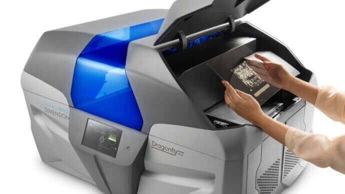
Of course, these advancements are getting their fair share of attention – just recently, Nano Dimension received a grant approval from Israel’s Chief Scientist worth up to $1.3 million to support the development of the DragonFly 2020 PCB 3D printer – the first inkjet 3D printed dedicated to printing multi-layer PCBs at home.
This is the second consecutive year in which Nano Dimension have received financial support from the Israeli government. The company also raised an initial $10.9 million in financing in June, along with investment agreements totaling $2.2 million in November.
It’s clear that the interest and demand for 3D printing electronics is high, as we’ve already seen this year with Voxel8 receiving financing for 3D electrical printers too. Watch this space for the future of 3D printing!
License: The text of "Nano Dimension: 3D Printing Multi-material Electrical Conductors" by All3DP is licensed under a Creative Commons Attribution 4.0 International License.